 TRUMP
TRUMP ETH
ETH BTC
BTC XRP
XRP SOL
SOL TAO
TAO TONCOIN
 STORY
STORY WLFI
WLFI RICH
RICH DEV3
DEV3 ATTN
ATTN


Untilization and Advantage of Standard PCB Panel Size

The PCB Panel advantage
A composite of published circuit card, i.e. Printed circuit boards that are not isolated are firmly repaired and also the setting up of the printed motherboard also comes from it, is typically taken as a published motherboard advantage. The charm of the design styles have to be the style of the published motherboard usage, in order to be able to utilize the published circuit card at optimum expenses and stocks and also arrangements. The impact of the PCB advantages on the production expenses of the PCB and the expense of assembly. The manufacturing expenses of published circuit boards become clear through the PCB panel examination control, which is the right law of the manufacturing panel with the control used by the printed circuit boards.
In the created instance in Figure 1, the lots on panel A (6-fold usage) is approx. 50% and also the lots on panel B (4-fold use) is approx. 70%.
With suitable individual printed circuit boards and also by skillfully dimensioning the panel and also preparing the panels appropriately, panel utilization of up to 85% can be achieved.
Number 1: PCB Panel use
pcb panel usage
Figure 2 reveals the family member expense payments in the production of printed motherboard for a conventional printed motherboard (100 * 160mm, 8 openings per cm2, 127µm track width/distance, surface area: HAL) depending upon the variety of layers. Essentially, only the costs for boring, cutting (racking up or milling), the electrical examination, packaging as well as for some material elements are straight depending on the number of printed circuit boards that can be suited on a panel. The continuing to be expense elements are independent of the number of printed motherboard per panel.
Figure 2: Expense elements in the production of printed circuit card
pcb parts
Normally speaking, it can be stated that approx. 70% to 80% of the PCB production costs are to be regarded as dealt with expenses, i.e. they are independent of the number of PCBs per panel. For the arrangements displayed in Number 1, this implies that the 8 circuit card (Panel B) can be made and also bought practically at the overall price of 6 circuit card (Panel A). The ideal advantage dimension in terms of producing prices is certainly dependent on the manufacturer. However, thinking about the commercially readily available panel cuts of 610 * 530mm or 1070 * 1225mm (typical sheet format) and the mounting margins and spacing needed for the manufacturing process, the PCB panel application and thus the price development in the PCB manufacturing for numerous PCB suppliers is an optimum advantage size of approx. 245 * 285mm.
The setting up process has cost components that are straight related to the number of parts per benefit as well as thus to the variety of printed motherboard per benefit, such as:
Intake of solder, direct SMD or THD setting up prices per element as well as AOI cost per part.
The expenses for packaging the circuit boards, an electric function test and for dividing the circuit card from the panel are symmetrical to the number of circuit boards in the panel. Other price elements are nearly independent of the number of printed motherboard in operation or the variety of parts on the published circuit card:
Throughput time of the benefit in the soldering system,
Time for paste printing,
The placement maker is idle throughout retraction/extension or adjustment of use.
Assembly prices for PCBs advantage
Figure 3: MOKO Printed Circuit Board Assembly expenses
pcb assembly
This decreases the processing costs in the PCB setting up for a benefit with an enhancing number of PCBs in the benefit, as displayed in concept in Figure 3. The following briefly analyzes whether taking full advantage of the number of published circuit card in terms of use is constantly highly sensible.
PCB Advantage Capacities
The optimum advantage size or PCB size differs depending upon the PCB maker and also technological tools. Based on the standard PCB panel size reduced 610 * 530mm, which is commonly processed, there are optimal dimensions of approx. 570 * 490mm for many producers. In electronic devices production at CAD-UL, the optimum dimensions are defined by the equipments made use of, supplied that it is to be carried out totally mechanically:
Paste printer 600 * 600mm
SMD choose and also put machine 400 * 550mm
Vapor phase soldering system 550 * 600mm
The following reasons oppose the processing of advantages with the optimum dimensions:
As PCB panel size boosts, this also loses stability, which can additionally be seen depending on the PCB thickness. There is a threat that the connection factors between the circuit card break because of incorrect handling.
The base materials for published circuit boards can diminish or extend throughout the published motherboard production procedure (dimensional stability). In addition, there are naturally manufacturing resistances in the manufacturing process of the circuit board, which can result in an offset of copper structuring, to boring and also contour of the circuit board as well as to a balanced out from layer to layer. With a lot of know-how and also by adjusting the manufacturing data, the PCB suppliers handle to keep the results to a minimum. With huge circuit boards or with large benefits where components with little pads, e.g. B. 0.4 mm pitch, positioned much apart, this can bring about borderline distinctions between the x, y placements of the pads on the circuit boards and also the connected outbreaks of the steel stencils for paste printing.
Extra actions have to be taken to prevent the bending of the PCB panels during transport in the transport gadgets, throughout paste printing, in the positioning system as well as throughout the soldering process. The flexing can result in faulty paste printing or mechanical stress on the solder joints.
In the manufacture of published circuit boards, troubles with the last assessment and also the electrical test emerge with raising measurements.
If there is a requirement not to permit failing motherboard in the panel, making best use of the variety of motherboard in the panel can result in a significant loss in return as well as hence to a price rise for the solitary motherboard.
Connection of the motherboard as well as benefit separation
The style of the advantages need to be reevaluated and also specified during the PCB layout stage to make sure that there are no surprises later throughout the assembly process. Generally, a choice for a treatment need to be made: scoring, milling or a mix of both. The setting as well as orientation of the components about the scraping trench or the milling ridges have to be picked so that the force used when the panels are divided is as tiny as possible. The copper needs to be set back adequately from the scoring trenches or perforation holes for the burrs to avoid water direct exposure. Ultimately, the design developer is additionally responsible for sufficient security of use during all machining processes and for the joint and coordinated optimization of the manufacturing and also setting up costs of the printed circuit card.
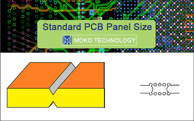
Connection of printed circuit boards as well as advantage splitting up for printed motherboard with a straight and continual shape with a minimum of two opposite parallel sides see Figure 4 and if there are no special needs when it come to border roughness, the scoring or notch milling process can be used. Trenches existing one over the various other are carved on both sides of the printed circuit card. The notch angle is normally 30 ˚, the notch depth depends upon the board thickness and the continuing to be core thickness is about 0.4 mm. The scribing process is no longer helpful for motherboard thicknesses above 2.0 mm. In order to reduce the mechanical anxiety when separating the published circuit boards from the panel to a minimum, CAD-UL utilizes a scratch PCB panel separator with a dealt with as well as a roller blade.
Number 4: PCB Rating advantages
For circuit card with uneven contours or if there are boosted demands concerning side roughness as well as dimensional precision, see Number 5, the circuit card shape need to be grated. The size of the milling cutters, normally 2.0 mm or 2.4 mm, for side processing must be defined due to the fact that the blanking procedure must be set to this milling size. Bars should stay throughout milling in order to connect the motherboard to each other or to the utility frame. The number, setting, as well as width of the internet must be thoroughly figured out depending upon the use or milling benefits of the published circuit board dimension and also density, in order to have the ability to assure adequate mechanical stability during all processing operations, along with to divide the published circuit card from the usage with little mechanical To be able to perform stress and anxiety on the solder joints and also parts. The internet can likewise be scratched or provided with perforation holes inside, on or outside the circuit board shape, see Figure 6, in order to be able to better decrease the anxiety impact when cutting.
Figure 5: PCB Milling advantages
With CAD-UL, the webs are either punched out by a pneumatically working web separator with a hook knife, or the circuit card are divided from each other by milling. Depending on the splitting up process and the placement of the opening openings, sharp-edged remnants of the internet can stay on the motherboard, which can lead to injuries. These are to be removed after the separation.
Number 6: Variations of router bars
A common feature of all depaneling procedures is that the circuit board flaws at the splitting up factors because of the mechanical activity throughout the separation which forces are exerted on the elements as well as the soldering points. These can cause component defects, in particular hairline fractures in SMD ceramic capacitors. Under particular situations, these issues are not instantly noticeable or have no result, yet just lead to breakdowns of the influenced elements after a long period of time.
Mixed benefits are specified as advantages that integrate different published motherboard with the same layer structure and similar production modern technology. The motivation for this is clear, published circuit card are only billed when and just one paste printing stencil is needed for a published motherboard with SMD on one side. If, nonetheless, the Gerber data collection provides several parts lists and several choice & area information sets for the benefit, in which reference names might be designated greater than as soon as, these information collections need to be incorporated with initiative and also risk of error by the job prep work department for electronic devices production in order to efficiently develop elements shopping and also to be able to successfully take into consideration the benefits as a setting up job. The majority of the moment, the various published motherboard are set up in the tool in one tool and these published circuit card are therefore required in the same number of items or in a set variety of pieces. Nonetheless, because raw circuit boards already stop working in use as well as mistakes can happen during the setting up of published circuit boards, the planned quantity proportion can not be ensured after the end of production. This can cause problems, especially with collection setting up. The savings in one-off costs at the start of the project may later be costly.
Figure 7: Combined benefit
All those entailed, the circuit board design, the motherboard supplier as well as the circuit card assembler ought to meticulously evaluate the benefits and also downsides of a mixed-use at the start of the task and also establish an ideal procedure with each other.
In order to make optimal use of the room on a manufacturing panel, it is additionally possible to utilize irregularly designed printed circuit card, e.g. L-shaped or T-shaped, to be arranged turned to each other on a PCB panel with 90 mit or 180 ˚. However, since published circuit card have preferred directions for paste printing as well as wave soldering, it ought to be checked whether this procedure likewise guarantees an optimum assembly process.
Lastly, a published circuit card that is to be produced and constructed separately, e.g. Elements put as well near the edge or where there disappears room for fiducial brand names as well as which therefore must be supplied with a receiving side on a minimum of 2 opposite sides are described as advantages
Please do not wait to call us if you have any type of questions concerning the design of the advantages or assistance in the creation of the advantages. Our staff members in the locations of PCB format and job preparation are constantly at your side with suggestions and also activity.
Dimensions of solitary motherboard as well as shipment benefits.
Single PCB
Please pick this choice if your circuit card contains a solitary circuit pattern. We always mill specific motherboard. The motherboard may contain interior cutouts as long as it does not separate the circuit layout. Otherwise, we speak of a PCB advantage.
If your PCB is smaller sized than 30x15mm, please put it in a shipment advantage. For this, we offer you the alternative “PCB Delivery advantage with on-line setup”.
Distribution benefits
Distribution benefit from file or plan:
The same relates to multi-use if you want to get various conductor patterns in one usage.
Delivery advantages with online setup:
Do you have the data of a single circuit card as well as no advantage drawing, yet want to have your motherboard in the delivery benefit? After that just inform us in the configurator exactly how we can design the advantages. If you need fixed breaking openings, please bring them right into the single picture in advance.
You can locate a lot more on the definition of a shipment advantage in our tutorial!
Enrollment marks in the side of the sheet
On demand, we can introduce enrollment marks in the delivery location of your printed circuit boards. Put it like 3 copper pads with a diameter of 1.00 mm in the middle of the side of the PCB panel. In the solder mask, these are excused with 2.00 mm.
Bitter pills in the distribution benefit
In the delivery benefit, it can take place that individual circuit boards are set out by our quality control if the top quality does not meet our standard. We never repaint greater than 50% of the printed motherboard on a distribution advantage. We also fill in the missing variety of products by sending even more distribution advantages than you got. To ensure that you constantly get at the very least the wanted number at the end.
Features of flex PCB
A circumferential edge of ≥ 7.50 mm is definitely necessary. If there is a copper-free surface, the delivery benefit edge is always rostered onto the top and bottom. This protects against the PCB from bending. The edge of the delivery benefit is always covered on both sides with flex lacquer (even with a 1F structure).
General details on measurements
The dimension of your motherboard is determined by the measurement from center shape to facility shape. We, therefore, advise utilizing a contour line of 200 µm to prevent ambiguities.
At Moko Technology, your printed circuit card can be machined making use of notches, milling or a mix of notches as well as milling. We perform milled PCBs.
When grating a multiple-use, your published motherboard continues to be connected in the benefit by means of preserving bars. The basic cutters are 1.60 mm, 2.00 mm or 2.40 mm.
When notching, we put your published motherboard in the distribution benefit.